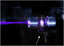
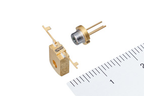
 Tohoku University and Sony Corporation announced that they have created a blue-violet wavelength ultrafast pulsed semiconductor laser with peak output levels 100 times of what is currently available.
According to the statement, this advance may enable a wide range of future applications including the development of very high capacity optical storage discs.
For more information visit: www.sony.net
Unedited press release follows:
Tohoku University and Sony Corporation jointly develop the world’s first*1 blue-violet ultrafast pulsed semiconductor laser with 100 watt output
– The path to practical light-source in next-generation large-capacity optical disc storage & for nano-fabrication –
Tohoku University
Sony Corporation
Professor Hiroyuki Yokoyama of the New Industry Creation Hatchery Center (NICHe), Tohoku University (hereafter, ‘Tohoku University’), and Advanced Materials Laboratories, Sony Corporation (hereafter, ‘Sony’), have succeeded in jointly developing a blue-violet ultrafast pulsed semiconductor laser*2 with dramatically improved peak laser beam output levels that are 100 times that of the world’s current highest levels.
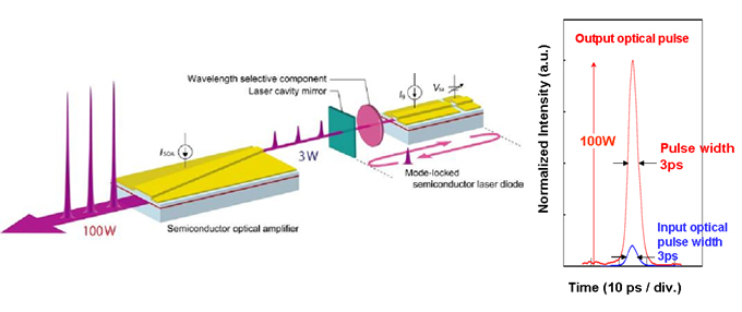
This latest successful development is an all-semiconductor laser picosecond pulse source with a laser wavelength of 405 nanometers (1 nm = one-billionth of a meter) in the blue-violet region. It is capable of generating optical pulses in the ultrafast duration of 3 picoseconds (1 picosecond = one-trillionth of a second), with ultrahigh output peak power of 100 watts and repetition frequency of 1 gigahertz. Advanced control of the newly-developed and proprietarily-constructed GaN-based mode-locked semiconductor laser*3 and semiconductor optical amplifier*4 have enabled peak output power in excess of 100 watts to be achieved, which is more than a hundred times the world’s highest output value for conventional blue-violet pulse semiconductor lasers.
Although there have been ultra high-output laser devices combining solid-state lasers*5 and a second harmonic generation unit for high functionality and high-value leading-edge chemical research applications in the past, the light source box itself was bulky and a specialist technician was required to ensure the stable operation of the laser. There are high expectations that this newly-developed semiconductor laser system, which incorporates semiconductor diodes, can have a much wider range of future applications. For instance, this technology enables the size of components such as the light source box to be drastically reduced.
This newly-developed ultra high-output, ultrafast pulsed semiconductor laser light source is capable of using a nonlinear optical process known as two-photon absorption*6, which occurs only as a result of high intensity optical pulses. When light from the laser beam is concentrated on the lens, it creates chemical and thermal changes in the vicinity of the lens focus spot which is narrower than even the diameter of the focus spot of the lens itself. It is anticipated that application of these properties will be possible in a wide range of fields such as three-dimensional (3D) nano-fabrication of inorganic/organic materials in the order of nanometers, and next-generation large-capacity optical disc storage.
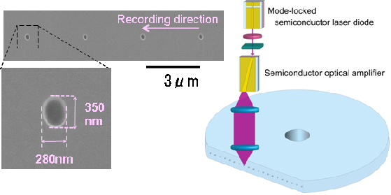
Sony tested the principles for applying this technology in next-generation large-capacity optical disc-storage by creating void marks with a diameter of approximately 300 nanometers at intervals of 3 micrometers on the interior of plastic material, and successfully read these marks with the laser beam.
These experimental results have been achieved through integration of Tohoku University’s fundamental technology on ultrashort pulse lasers (Tohoku University is promoting joint research program for industry-academic collaboration based on materials and devices), and Sony’s fundamental technology on semiconductor laser diodes. Hereafter, Tohoku University and Sony will work to further develop its fundamental technology for creating even higher output and multi-functionality, while developing the practical applications of this technology to make these systems even more compact and stable.
These research findings were also published in the latest edition of the US academic journal, ‘Applied Physics Letters’. (Appl. Phys. Lett. volume 97, issue 2, page 021101 (2010); doi:10.1063/1.3462942 (3 pages), Online Publication Date: 12 July 2010 )
* Outline of the blue-violet ultrafast pulsed semiconductor laser system
* Temporal waveforms of light using streak camera measurement
* Performance characteristics of an experimental blue-violet ultrafast pulsed semiconductor laser
Laser wavelength: 405 nm (GaN-based semiconductor laser)
Peak optical output: 100W or more
Repetition frequency: 1 GHz
Pulse width: 3 ps
* Testing the principle of optical disc storage using an experimental laser
<Explanation of Annotations>
*1 :Information current as at July 20th, 2010, and as investigated by Tohoku University and Sony.
*2 Ultrafast pulsed semiconductor laser: A semiconductor laser capable of emitting pulsed laser beams (repeated blinking at short intervals), where each pulse duration is extremely short (3 picoseconds in this case).
*3 Mode-locked semiconductor laser: A type of semiconductor laser that emits ultrafast optical pulses. It operates by sending optical pulses with an ultrafast duration in the order of picoseconds (or less) back and forth within the laser cavity.
*4 Semiconductor optical amplifier: An optical amplifier that can amplify the laser beam directly using a semiconductor. Although the structure is similar to that of a semiconductor laser, the beam-amplifying functionality is enhanced through antireflective fabrication of the laser facets.
*5 Solid-state lasers: Lasers that use solid crystals such as rubies as the laser medium. Mode-locked Ti: Sapphire lasers, which are representative of ultra-fast pulse / picosecond mode-locked solid-state lasers, use a sapphire crystal doped with titanium ions as the lasing medium.
*6 Two-photon absorption (TPA): This is a typical nonlinear optical process. When a substance interacts with extremely intense light, the substance does not always respond in proportion to the electromagnetic field of the light, thus creating a prismatic effect. TPA is the phenomenon of absorbing two photons simultaneously to excite the eigenstate corresponding to the resulting sum of photon energy. Using this phenomenon to focus light from an intense laser beam on a lens will result in an extremely high density of power in the vicinity of the focus point. Thus, when fabricating inorganic/organic materials using a laser beam, it becomes possible to perform three-dimensional fabrication by altering the focus point.


